Graphene Layered with Magnetic Materials Could Drive Ultrathin Spintronics
Tiny swirling textures in the magnetic fields within layered materials could be a key to replacing disk drives and flash memory in computing devices. Physicists at UC Davis and the Lawrence Berkeley National Laboratory are exploring how these patterns form in materials layered with graphene, an ultrathin form of carbon. A paper on the work was published online May 28 in Nature Materials.
Graphene is a form of carbon with the atoms arranged in a sheet one atom thick. Described as “the world’s thinnest material” it is essentially two-dimensional. It was discovered in 2004 by two researchers at the University of Manchester, England and has a number of potentially useful properties: for example, it is very strong, transparent and conducts electricity.
Physicists have been looking at the exotic magnetic properties of layered materials for some time, but the concept of using graphene in them is quite novel, according to Gong Chen, co-first author on the paper, who started the project as a postdoctoral fellow in Andreas Schmid’s group at the Berkeley Lab and now a project scientist in Kai Liu’s group at UC Davis.
“It has only recently become a hot topic,” Chen said. “This effect in thin films had been ignored for a long time. This type of multilayer stacking is really stable and robust.”
In the new study, Chen and colleagues coupled graphene with thin layers of magnetic materials like cobalt and nickel. The team performed key measurements at Berkeley Lab’s Molecular Foundry, a nanoscience research center.
They looked at the “spin” behavior within the materials. Think of spin as the orientation of many tiny compass needles within the material. The spin property is affected by the interaction of graphene with the other magnetic layers, they found.
The experimental work was performed in close collaboration with theoretical efforts led by Hongxin Yang and Mairbek Chshiev at the Grenoble Alps University, France, and Nobel Laureate Albert Fert, emeritus professor at Paris-Sud University, France. Fert shared the Nobel Prize in Physics in 2007 for his discovery of the giant magnetoresistance effect that led to novel ways of utilizing electron spin for information storage, including technology for reading data in hard drives.
Spintronics in ultrathin materials
The researchers found that the material’s electronic and magnetic properties create tiny swirling patterns where the layers meet. This effect gives scientists hope for controlling the direction of these swirls and tapping this effect for a form of spintronics applications known as “spin-orbitronics” in ultrathin materials. The ultimate goal is to quickly and efficiently store and manipulate data at very small scales, without the heat buildup that is a common problem for miniaturizing computing devices.
Typically, researchers have worked with heavy and expensive metals like platinum and tantalum to achieve such effects. Graphene offers a potentially revolutionary alternative since it is ultrathin, lightweight, has very high electrical conductivity and can also serve as a protective layer for corrosion-prone magnetic materials.
The next step is to find ways to control tiny swirls in the magnetic texture of the material, called skyrmions. These miniature magnetic vortices can rotate either clockwise or counter-clockwise. In materials science, that property is called chirality. Understanding how to control or amplify that magnetic chirality would be key to developing these materials into new devices that can store, retrieve and process data.
The results open up an unexpected new direction to explore spin-orbitronics in graphene and other two-dimensional systems, said Kai Liu, coauthor on the paper and a physics professor at UC Davis.
“For example, it allows us to explore topological characters of the spin texture which have potentials for low power nanoelectronics, while taking advantage of a host of exotic properties of graphene,” Liu said.
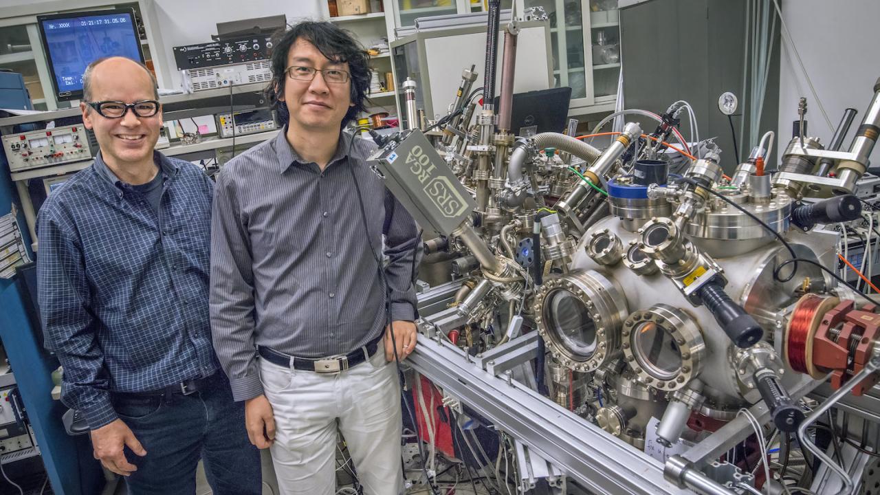
To measure the layered material, Chen used spin-polarized low-energy electron microscopy (SPLEEM) at the Molecular Foundry’s National Center for Electron Microscopy, together with Andreas Schmid and other co-workers. It is one of just a handful of specialized devices around the world that allow scientists to combine different images to map a sample’s magnetization profile in three dimensions, revealing its “spin textures.”
These researchers are now working to form the graphene-magnetic multilayer material on an insulator or semiconductor to bring it closer to potential applications.
Researchers from Paris-Sud University, a joint center that includes the French National Center for Scientific Research, Thales Physics Lab, Paris-Sud University, and Paris-Saclay University in France; the Chinese Academy of Sciences; Nuclear Technology Development Center (CDTN), Federal University of Minas Gerais, and Federal University de Lavras in Brazil participated in the study.
The work was primarily supported by the U.S. Department of Energy Office of Basic Energy Sciences; the European Union’s Horizon 2020 Research and Innovation Program; the US National Science Foundation; and the University of California Office of the President Multicampus Research Programs and Initiatives.
More information
Significant Dzyaloshinskii–Moriya interaction at graphene–ferromagnet interfaces due to the Rashba effect (Nature Materials)
Adapted by Andy Fell, UC Davis News Service, from a story by Glenn Roberts Jr., writer with the Lawrence Berkeley National Laboratory. Read Glenn’s original story here.
